Semiconductor manufacturing
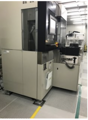
We provide contract manufacturing service of semiconductor IC assembly mainly for Image sensor. Our assembly team had originally belonged to FUJIFILM Optics, one of the best digital camera brand company. Major assembly process operates under the best-in-class quality clean room Class 100. Additionally, we can support multiproduct lines from small volume productions. Class 100 makes high quality & low-yield level production environments.
Over 30 years of Image sensor production experiences, and a member of the Kanematsu group network in the world, which enable us to offer customers a wide range of assembly services for Image sensor, include custom designs, testing & inspections which collaborate with outsourcing companies.
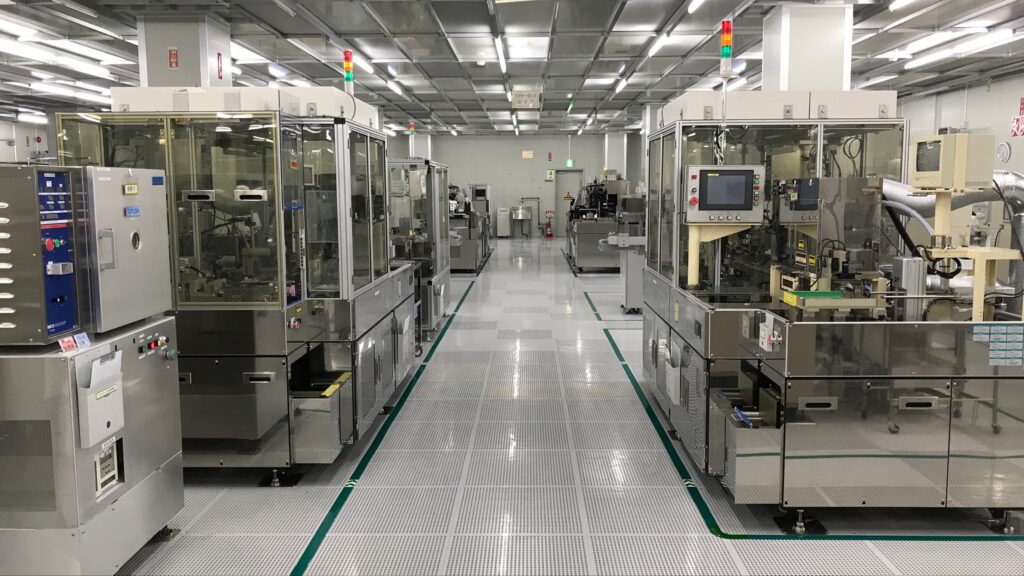
Class100 Clean room
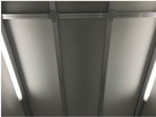
HEPA Filter
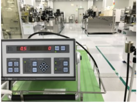
0.5um Zero Particle
Down Flow Structure
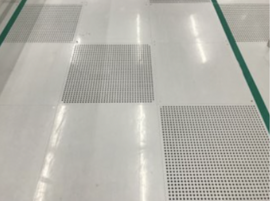
Image Sensor Package Variations
| Ceramic Package | iBGA | Transparent Mold |
|---|---|---|
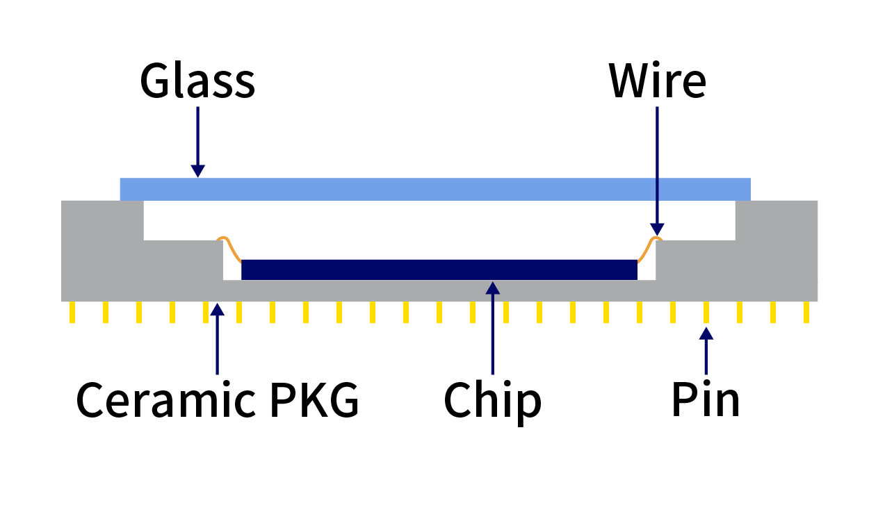 KFT | 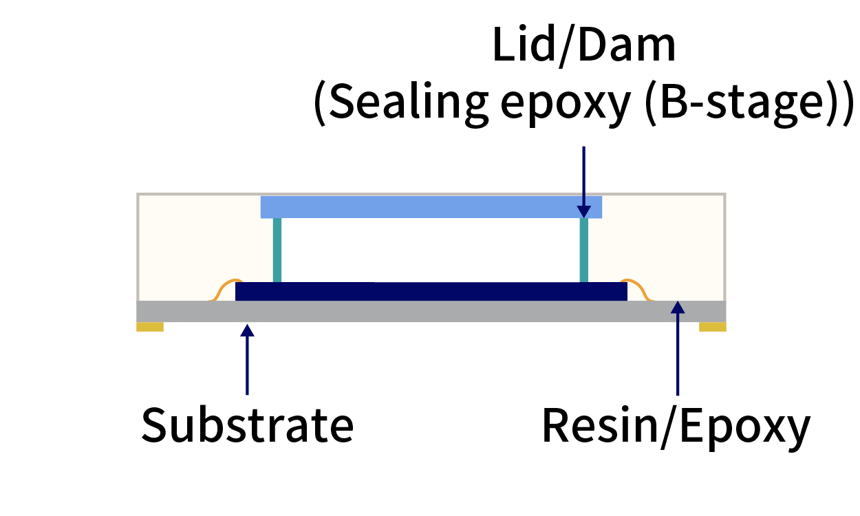 Outsource | 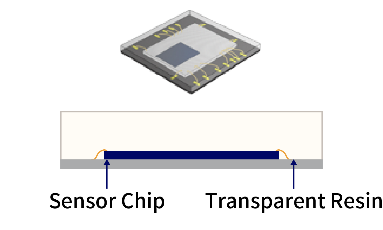 Outsource |
| COB(Chip on board) | iCSP | |
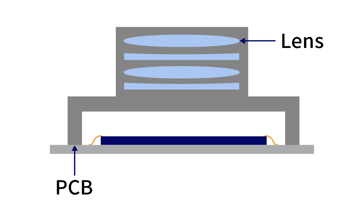 KFT | 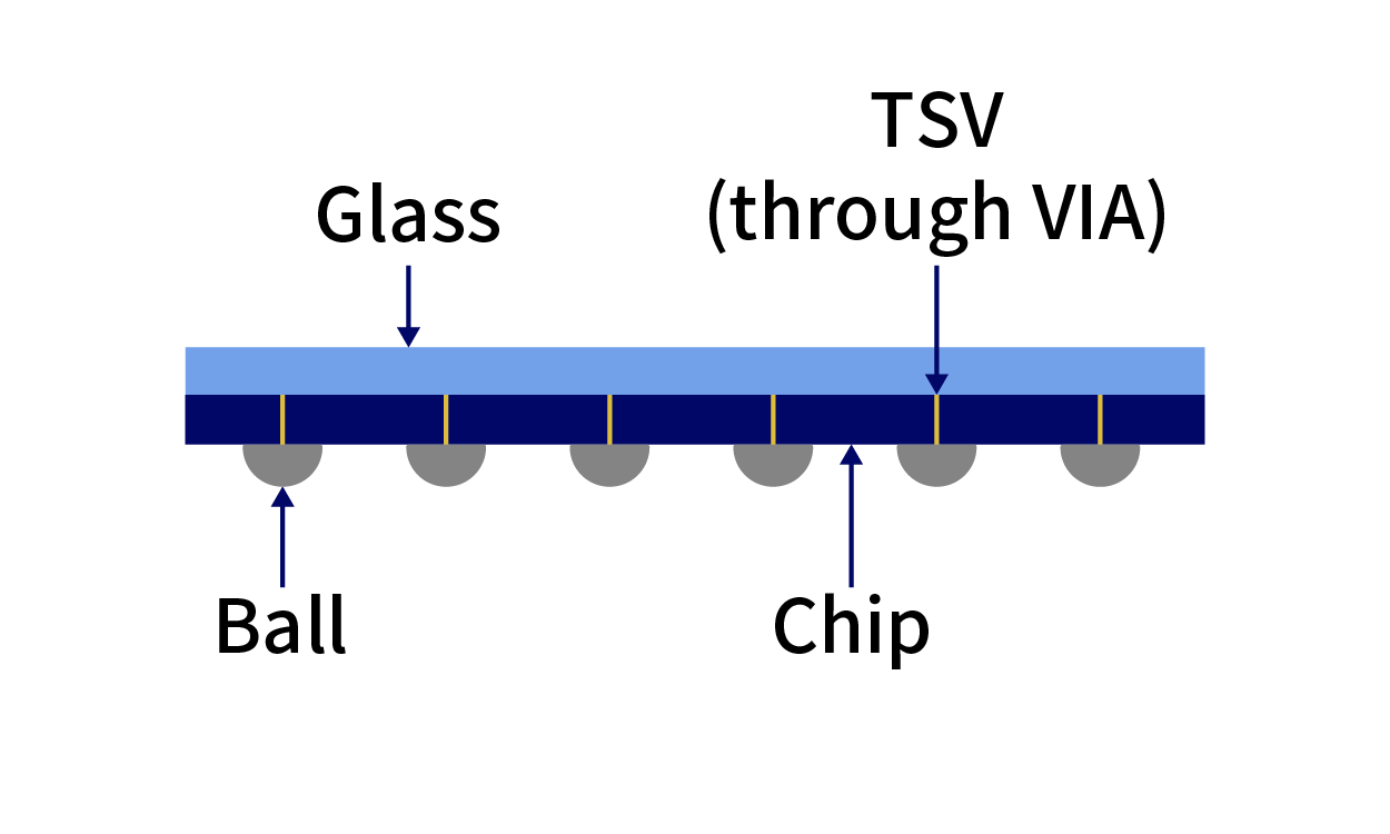 Outsource | |
| *Depends on Technical requirement | ||
Major Process of Image Sensor Assembly
This is our major process of Image sensor assembly. We can also support additional process as per based on requests.
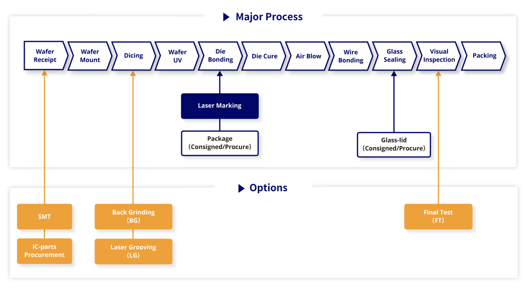

Both of 8 inch(200mm) and 12 inch(300mm) can be handled. After receipt, wafer will be stored in desiccator in class 100 clean room.

Mount wafer on a dicing tape without surface damage and contamination. Wafer backgrinding(BG) can be done as customer requirement.

Chips(dies) are separated from a finished wafer. Choose suitable blade and speed setting to avoid contamination by silicon powder and chipping.

Adhesion lowering process to enable to pick up chips(dies).

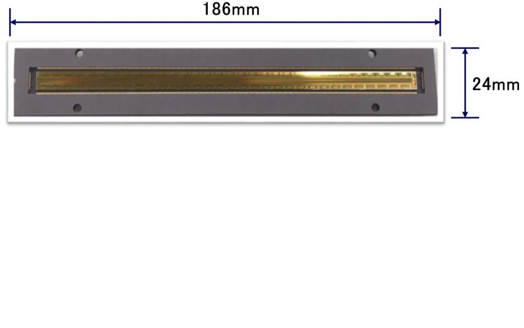
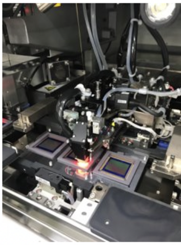
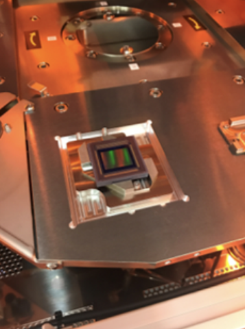
Attach chips(dies) to package with high accuracy. KFT can handle various chip(die) size, max. 70*70mm for area sensors and max. 170mm for line sensors.

Apply heat to cure die bonding adhesive.

Clean before glass sealing.
Connect electrodes of chip(die) and package with gold wire(Au). Min. 60*60um can be handled.

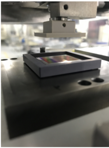
Seal by glass to avoid contamination.
KFT can accommodate sealing method, such as UV sealing, heat curing, and tape fastening, according to customer requirements.

Inspect defect such as contamination in sealed area, stain, wire defect and visual defect.

Shipping assembled sensors with moistureproof packing.
Major Process
Dicing
Die-bonding
Wire-bonding
Glass-sealing
Production Record
Biggest Area-sensor

Longest Line-sensor